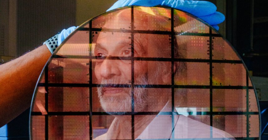
Subramanian Iyer, an electrical engineer and educator, has long specialized in a sleepy niche of the semiconductor industry that has now become a major choke point in the global contest for artificial intelligence leadership.
That niche is a technology called advanced chip packaging, which bundles as many as dozens of the components in palm-size modules. As computing gains from the traditional practice of shrinking transistors to pack more of them onto each chip have diminished, Nvidia and other chip giants have turned to packaging as an essential way to deliver semiconductors capable of more complex tasks for A.I.
Dr. Iyer, 72, a former IBM technologist and now a professor at the University of California, Los Angeles, has helped drive packaging advances over decades. But he and chip industry executives have watched in alarm as U.S. leadership in the field has slipped away to the same company that dominates advanced chip manufacturing.
Taiwan Semiconductor Manufacturing Company, which makes cutting-edge chips for Nvidia and other A.I. leaders, also packages nearly all of them. Its key suppliers and partners are mainly in Taiwan, too, facing the same threat from China that caused U.S. policymakers to funnel billions of dollars into boosting domestic chip fabrication.
The packaging bottleneck has become a hot topic in Silicon Valley as TSMC has struggled to keep up with demand. Dr. Iyer tried to help by developing plans for a packaging research and development center, funded with $1.1 billion from the Biden administration and slated to be built in Arizona, but the Trump administration effectively killed the effort last year.
“The bottom line is they’ve thrown the baby out with the bathwater,” Dr. Iyer said. “We’ve ended up in a place where we are even more dependent on TSMC.”
The bottleneck underlines how U.S. dependence on Taiwan has not eased despite efforts by the Biden and Trump administrations. The Biden administration allocated more than $50 billion to jump-start domestic chip production under the 2022 CHIPS and Science Act. President Trump, objecting to grants to chip makers, has instead pressed for deals with U.S. companies that include equity stakes and threatened foreign companies with tariffs to essentially accomplish the same thing.
After the making of chips, “packaging is the most important thing,” said Patrick Gelsinger, Intel’s former chief executive, who lobbied for the CHIPS Act. “And our packaging supply chains may be even more precarious.”
A Trump administration official disputed that packaging was not a top priority. Nine packaging manufacturing projects have received CHIP Act funding, and the Commerce Department is evaluating some important research projects in the field, the official said, speaking on the condition of anonymity.
To break through the logjam, some big U.S. companies are trying to step up. Intel, a longtime leader in the technology, has picked up packaging customers and said last week that it had recruited a new executive to lead advanced packaging. Applied Materials, the biggest maker of chip manufacturing tools, is building a $5 billion research facility in Silicon Valley with partners, with packaging as a key sideline.
Amkor Technology, a packaging specialist, is building its first U.S. factory site in Arizona and is expected to take on some packaging work for TSMC under a 10-year deal. Amkor, which the Biden administration awarded a $407 million grant, boosted its own potential investment on the site to $7 billion after talks with Trump administration officials and signs of purchasing interest from Nvidia and Apple.
Such customers are showing “very strong demand, wanting to build a U.S. ecosystem,” said Kevin Engel, Amkor’s president and chief executive.
Packaging was long considered an afterthought that U.S. chip makers farmed out to countries in Asia with low wages. The U.S. share of chip packaging is around 3 percent, according to the Global Electronics Association.
Chips don’t work without packaging. The process, also called assembly, typically wraps bare pieces of silicon in protective plastic with connectors to pass signals to other chips on a circuit board.
These days, chips are frequently placed on an intermediary layer called a substrate, which is typically made of plastic and glass fiber and embedded copper wiring.
Dr. Iyer, who earned a doctorate at U.C.L.A. before joining IBM in 1981, pushed another key advance. At IBM, he developed one of the first “interposers,” a layer made from silicon that holds multiple chips side by side and sends signals between them at greater speeds.
For the larger packages that some A.I. processors need, TSMC and Intel embed small pieces of silicon in substrates to act as communication bridges between chips.
“You can’t make them without advanced packaging,” said Mark Gardner, an Intel vice president and general manager for packaging and testing. “We’d be in a very different place in the A.I. world without it.”
TSMC offers advanced packaging called CoWoS, short for chip on wafer on substrate. Nvidia’s new Rubin processor, for example, uses CoWoS to bundle two large A.I. chips with eight stacks of high-speed memory that each contain 12 chips, amassing 336 billion transistors in one package. By 2029, TSMC predicts a 48-fold boost in computing transistors per package compared with 2024.
But the company, which received CHIPS Act funding to build major chip factories in Arizona, doesn’t plan to use CoWoS in the state until 2028 or 2029. Any chips it makes there now must be sent to Taiwan for packaging.
TSMC is already struggling to catch up with A.I.-driven orders. Its CoWoS production is about 30 percent short of demand, estimated Handel Jones, an analyst at International Business Strategies, who said TSMC accounted for about 95 percent of all advanced packaging.
“All I see is demand continuing to go higher and higher,” said Kevin Chang, a TSMC senior vice president. “It is certainly going to cause a lot of constraints.”
And costs remain high. An advanced chip package may cost $500, said Jan Vardaman, president of the research firm TechSearch International. Simpler packages may cost closer to $40, industry executives said.
Some chip start-ups are deliberately avoiding designs relying on CoWoS, which can require months to design the required interposer.
“Didn’t want to touch it,” said Sha Rabii, a co-founder and the president of Majestic Labs, which is designing an A.I. processor that can use simpler packaging and cheaper memory chips. “It takes a key part of the supply chain challenge off the table.”
Over the long term, Dr. Iyer and industry executives said, there need to be new packaging concepts. Syenta, an Australian start-up, has proposed one that uses electrochemical techniques to create extra-large packages with fewer manufacturing steps and up to a twentyfold boost in communications bandwidth, said Jekaterina Viktorova, the company’s chief executive.
Others are marshaling partners for packaging research. Resonac, a Japanese chemical maker, recently announced a 12-company packaging consortium and pilot production line near Silicon Valley.
But government support remains uncertain. The Biden administration had designated a nonprofit, Natcast, to oversee $7.4 billion in research funding from the CHIPS Act, with packaging as a focus candidate.
In 2023, Dr. Iyer joined the Commerce Department’s chip program, devising a plan for a facility where researchers could develop and test new semiconductor materials, chips and packaging. He returned to U.C.L.A. in the fall of 2024.
The Commerce Department didn’t announce the facility’s proposed funding and location, at an Arizona State University research park, until January 2025. Under Mr. Trump, there was little action until Commerce Secretary Howard Lutnick declared that Natcast was an illegally created organization that August and clawed back its funding. The group disputed that claim but disbanded last fall.
Not all industry executives are mourning the would-be Arizona packaging facility. Mr. Gelsinger, now a general partner at the venture capital firm Playground Ventures, contends it should have been at an existing research facility rather than started from scratch.
Dr. Iyer, who wasn’t involved in the site selection, agreed. But he added: “I thought I put together a good program. I did not expect it to fall apart.”